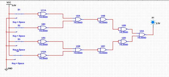
Activity 2.3.3 - Multiplexers / Demultiplexers
Building off of 2.3.2 - Seven Segment Displays, work on completing activity 2.3.3 including its conclusion questions. Circuit Current and Power calculations should be done individually, as should the circuit simulations in multisim.
|

|

|

|
Conclusion Questions
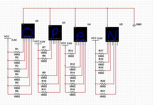
1.As discussed in the Procedure, the un-multiplexed version of the circuit that displays the word OPEN uses 1.89 watts of power. On average, how much power does the multiplexed version use? For the sake of simplicity, you may assume that the 74LS139 requires no power.
Only one display is on at any given time. 1.89 watts/4 = .47 W
Only one display is on at any given time. 1.89 watts/4 = .47 W
Activity 2.2.3 Universal Gates:
NOR Only Logic Design
In this activity you will revisit the voting booth monitoring system introduced in Activity 2.2.2 NAND Logic Design. Specifically, you will be implementing the NOR only combinational logic circuits for the two outputs Booth and Alarm. In terms of efficiency and gate/IC utilization, these NOR only designs will be compared with the previously designed AOI and NAND implementations.


|


|
Activity 2.2.2 Universal Gates NAND Logic Design
In this activity you will implement NAND only combinational logic circuits for the two outputs Booth and Alarm. These NAND only designs will be compared with the original AOI implementations in terms of efficiency and gate/IC utilization. In a future activity, these NAND only designs will be compared to the circuits implemented using only NOR gates.


|


|
Conclusion Activity 2.2.2 + 2.2.3 NAND and NOR

Using only NAND gates to make all the gates needed would make it easier to make, and chaper to buy many NAND gates to make all the circuits.
I think that different chips could have been used for this design which would have made it need less gates to work and would have made it more efficient.
The Nor and the AOI are similar and can compare to each other. It only uses nor gates making it really efficient and better when buying chips and soldering the circuits together.
The NAND and NOR implementation is almost the same and the efficiency only changed because of the number of OR and AND gates. Because there is a different way of making the OR and AND gates using the NOR and NAND gates.
2.1.3 AOI Logic Implementation

|

|

Activity 1.2.6 The 555 Timer
In this activity you will simulate and build a 555 Timer oscillator. You will observe the effect that varying the value of its resistor and capacitor values has on the oscillation frequency and duty cycle.

Activity 1.2.4 Sequential Logic Design (DMS
In this activity we will use the D flip-flop introduced in the previous lesson. We are limiting our use to this type of flip-flop in this introductory unit because of its simplicity and ease of use. The D flip-flop is just one of many different types of flip-flops that can be used to implement sequential logic circuits.

|

|
Activity 1.1.8 Soldering Practice
The project you have just completed constitutes what is commonly known as a shift-register. In this project we practiced soldering and put it all together and tested it with a battery.

|

|
This is my soldering project. It was my first time soldering so it was a very fun experience. Before doing this project, I did not know what soldering was. This project was a very easy and fun. I made a couple mistakes during this project. but they were easily fixed. One of my mistakes is that I put the icchips on backwards but it was easy to take it off and put in on the right way. I also put the big resistor in the place where the small resistor was supposed to go but I did not change this because the teacher said that that it will still work. After finishing all of these steps I tested it with a battery and it worked. At first I was frustrated because it was not working but then it started working and I got happy. I think that before you start working on something you should plan ahead so you wont make a careless mistake. The big resistor that I put in place of the small resistor was a careless mistake and if I had to take it out it would have took a lot of time and more effort that should not be needed.
Activity 1.1.6 Component Identification: Digital
In this activity you will investigate both combinational and sequential logic gates. You will be asked to simulate simple circuits using basic logic gates. You will then complete a truth table for each logic gate based on the outputs generated from your simulation.

|

|

Activity 1.1.5 Circuit Theory: Simulation and Breadboard

|

|

|
This shows the Activity 1.1.5 with both of the parts the virtual bread boarding and the physical bread boarding. The reason that you can not see my virtual bread boarding on here is because tinker cad did not save my work. However I personally think that the virtual part was easier than the physical part. The physical part was easy at first but it got a little confusing with all the wires going everywhere. Asking my teacher for I help I worked through it and my pictures of the process are above this. I thought that I would get the same calculations but they were not the same. This project helped me work with breadboards more and be able to use them. I think that the next time we work with breadboards I will be able to use them a little better since I have previous knowledge with them. One thing that I learned during this project and I should take along as a lesson to be used on all my future projects in all my classes is to ALWAYS SAVE MY WORK.I learned this when my digital part of the breadboard project did not work. I enjoyed this project and really had fun doing it but the only part that got me angry is when I was confused and did not know what to do.
Activity 1.1.4 Component Identification: Analog

Activity 1.1.2 Investigating Basic Circuits

